
How Does PCB SMD Assembly Differ From PCB Fabrication?
PCB SMD Assembly Differ From PCB Fabrication
PCB smd assembly differs from a typical PCB fabrication because it doesn’t involve cutting the substrate into a specific form or shape. Instead, it involves mounting components onto the surface of the bare board to establish electrical pathways. This allows for the creation of an electronic device that can function as intended once it has been connected to a power source. To accomplish this, the bare circuit board is coated with an epoxy-based material that leaves designated spaces for attaching the necessary components. It also features a silkscreen layer that imparts essential component details, including reference designators and values. It is critical that this information remains legible throughout the assembly process to promote accurate placement and reduce error rates.
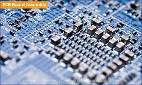
SMT stands for Surface Mount Technology, and it is a technology that eliminates the need to reserve through holes on the PCB for component pins. SMD components are much smaller than their through-hole counterparts, so they can be mounted closer together and more easily fit on the surface of the board. This method is preferred because it allows for a higher component density, which can improve the efficiency and functionality of the finished product. It also is more cost-effective than through-hole insertion.
Once the SMDs are in place, reflow soldering will occur. This involves sending the board through a furnace that melts the solder paste, and then passing it through coolers that gradually lower the temperature. This solidifies the solder and cements the SMDs in place.
The SMT assembly process requires the use of specialized machinery that is programmed to correctly identify and place each component on its assigned location. This ensures that every SMD is properly positioned on the PCB, allowing for an efficient and effective production process. The machine also utilizes special sensors to detect and correct errors that may occur during the assembling process, such as solder bridges or electrical opens.
How Does PCB SMD Assembly Differ From PCB Fabrication?
Once the requisite components have been properly placed on the PCB, it goes through a soldering process that is very similar to the reflow soldering technique used with THT. The circuit board is sent through a furnace, which melts the paste and helps it flow as needed. It then passes through a series of coolers that help the solder set and solidify. Once this is complete, the circuit board is inspected for any errors that have occurred.
In addition to detecting and correcting errors, the pcb smd assembly process must also be able to manage the amount of flux residue left behind during the soldering process. This is an important step because the residual flux can contaminate sensitive equipment or damage solder joints over time. Additionally, the flux residue can lead to a dingy appearance on the finished product, which can detract from its overall quality.
The pcb smd assembly procedure can be a messy and frustrating one because of the presence of flux residue and oil particles from human handling. This can cause a variety of problems, such as electrical opens, solder bridging, and “tombstoning” that can compromise the strength of the finished product. As a result, it is important to clean the PCB after each step of the assembly process.